- 您现在的位置:买卖IC网 > Sheet目录1992 > CY28410OXC-2 (Silicon Laboratories Inc)IC CLOCK CK410 GRANTSDALE 56SSOP
CY28410-2
......................Document #: 38-07747 Rev *.* Page 10 of 16
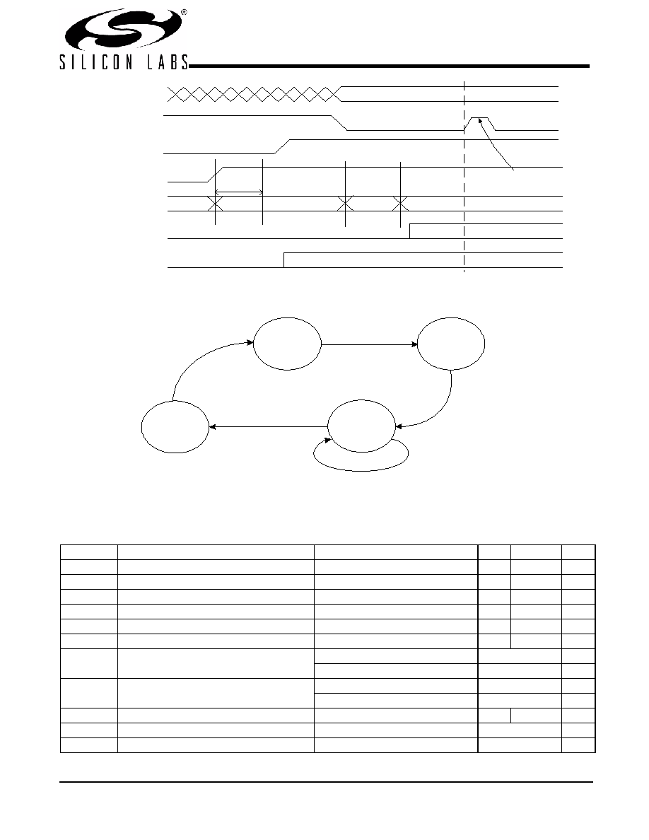
FS_A, FS_B,FS_C
VTT_PW RGD#
PW RGD_VRM
VDD Clock Gen
Clock State
Clock Outputs
Clock VCO
0.2-0.3m S
Delay
State 0
State 2
State 3
Wait for
VTT_PW RGD#
Sam ple Sels
Off
On
State 1
Dev ice is not affected,
VTT_PW RGD# is ignored
Figure 5. VTT_PWRGD# Timing Diagram
VTT_PW R G D# = Low
Delay
> 0.25m S
S1
Power O ff
S0
V D D _A = 2.0V
Sam ple
Inputs straps
S2
Norm al
O peration
W ait for <1.8m s
Enable O utputs
S3
VTT_PW RG D # = toggle
VD D_A = off
Figure 6. Clock Generator Power-up/Run State Diagram
Absolute Maximum Conditions
Parameter
Description
Condition
Min.
Max.
Unit
VDD
Core Supply Voltage
–0.5
4.6
V
VDD_A
Analog Supply Voltage
–0.5
4.6
V
VIN
Input Voltage
Relative to VSS
–0.5
VDD + 0.5
VDC
TS
Temperature, Storage
Non-functional
–65
150
°C
TA
Temperature, Operating Ambient
Functional
0
70
°C
TJ
Temperature, Junction
Functional
–
150
°C
JC
Dissipation, Junction to Case
(Mil-Spec 883E Method 1012.1)
SSOP
39.56
°C/W
TSSOP
20.62
JA
Dissipation, Junction to Ambient
JEDEC (JESD 51)
SSOP
45.29
°C/W
TSSOP
62.26
ESDHBM
ESD Protection (Human Body Model)
MIL-STD-883, Method 3015
2000
–
V
UL-94
Flammability Rating
At 1/8 in.
V–0
MSL
Moisture Sensitivity Level
1
发布紧急采购,3分钟左右您将得到回复。
相关PDF资料
CY28410OXC
IC CLOCK CK410 GRANTSDALE 56SSOP
CY28411ZXC
IC CLOCK CK410M ALVISO 56TSSOP
CY28442ZXC-2
IC CLOCK ALVISO PENTM 56TSSOP
CY28445LFXC-5
IC CLOCK CALISTOGA CK410M 68QFN
CY28446LFXC
IC CLOCK CALISTOGA CK410M 64QFN
CY28447LFXC
IC CLOCK CALISTOGA CK410M 72QFN
CY28547LFXCT
IC CLOCK CK505/410M INTEL 72QFN
CY28548ZXC
IC CLK CK505 960M/965M 64TSSOP
相关代理商/技术参数
CY28410OXC-2T
功能描述:时钟发生器及支持产品 SysClk Intel Lakeprt & Grantsdale Chipset RoHS:否 制造商:Silicon Labs 类型:Clock Generators 最大输入频率:14.318 MHz 最大输出频率:166 MHz 输出端数量:16 占空比 - 最大:55 % 工作电源电压:3.3 V 工作电源电流:1 mA 最大工作温度:+ 85 C 安装风格:SMD/SMT 封装 / 箱体:QFN-56
CY28410OXCT
功能描述:时钟发生器及支持产品 SysClk Intel Lakeprt & Grantsdale Chipset RoHS:否 制造商:Silicon Labs 类型:Clock Generators 最大输入频率:14.318 MHz 最大输出频率:166 MHz 输出端数量:16 占空比 - 最大:55 % 工作电源电压:3.3 V 工作电源电流:1 mA 最大工作温度:+ 85 C 安装风格:SMD/SMT 封装 / 箱体:QFN-56
CY28410ZC
制造商:SPECTRALINEAR 制造商全称:SPECTRALINEAR 功能描述:Clock Generator for Intel Grantsdale Chipset
CY28410ZCT
制造商:SPECTRALINEAR 制造商全称:SPECTRALINEAR 功能描述:Clock Generator for Intel Grantsdale Chipset
CY28410ZXC
功能描述:时钟发生器及支持产品 SysClk Intel Lakeprt & Grantsdale Chipset RoHS:否 制造商:Silicon Labs 类型:Clock Generators 最大输入频率:14.318 MHz 最大输出频率:166 MHz 输出端数量:16 占空比 - 最大:55 % 工作电源电压:3.3 V 工作电源电流:1 mA 最大工作温度:+ 85 C 安装风格:SMD/SMT 封装 / 箱体:QFN-56
CY28410ZXC-2
制造商:CYPRESS 制造商全称:Cypress Semiconductor 功能描述:Clock Generator for Intel Grantsdale Chipset
CY28410ZXC-2T
制造商:CYPRESS 制造商全称:Cypress Semiconductor 功能描述:Clock Generator for Intel Grantsdale Chipset
CY28410ZXCT
功能描述:时钟发生器及支持产品 SysClk Intel Lakeprt & Grantsdale Chipset RoHS:否 制造商:Silicon Labs 类型:Clock Generators 最大输入频率:14.318 MHz 最大输出频率:166 MHz 输出端数量:16 占空比 - 最大:55 % 工作电源电压:3.3 V 工作电源电流:1 mA 最大工作温度:+ 85 C 安装风格:SMD/SMT 封装 / 箱体:QFN-56